Electronic design automation (EDA) tools and third-party IP blocks are ready for TSMC’s performance-enhanced N2P and N2X process technologies (2nm-class), the world’s largest foundry announced at its European Open Innovation Platform (OIP) forum this week. This allows various chip designers to develop chips based on TSMC’s second-gen 2nm-class production nodes, thus taking advantage of nanosheet transistors and low-resistance capacitors.
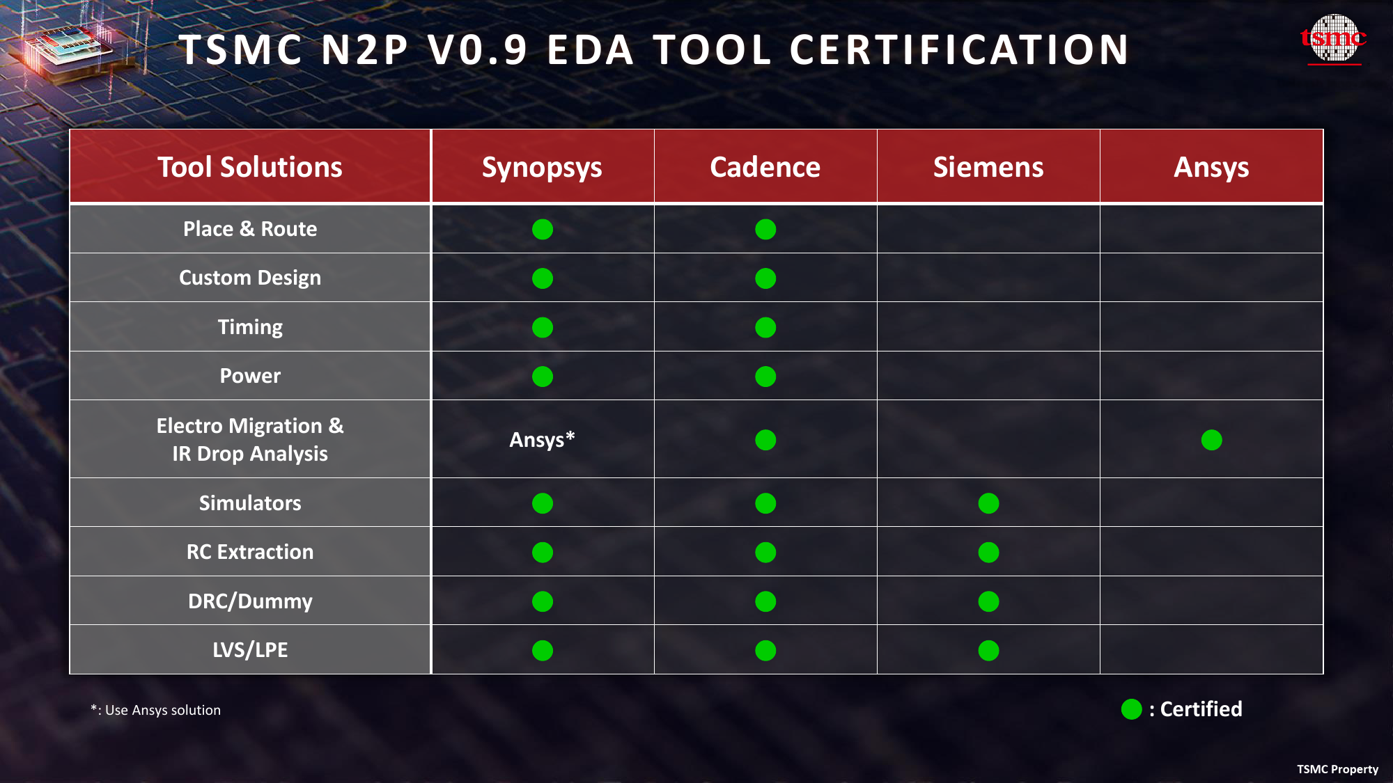
By now, all major tools from Cadence and Synopsys, as well as simulation and electromigration tools from Siemens EDA and Ansys, are ready for TSMC’s N2P fabrication process. These programs have already been certified for the N2P process development kit (PDK) version 0.9, deemed adequate as mass production using this fabrication process is slated for the second half of 2026, about two years from now.

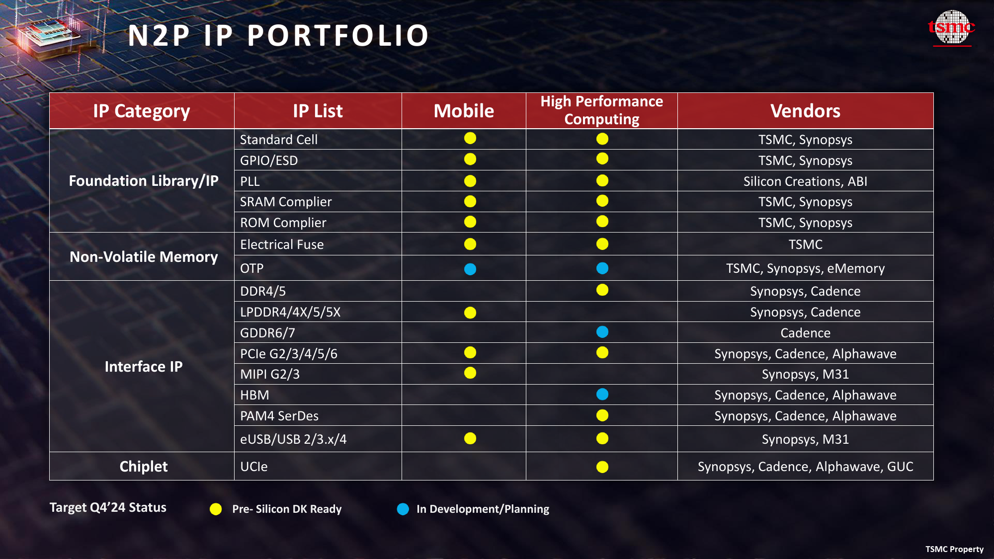
In addition, third-party IP, including standard cells, GPIOs, SRAM compilers, ROM compilers, memory interfaces, SerDes, and UCIe products, are now available in pre-silicon design kit form from various vendors, including TSMC itself, Alphawave, ABI, Cadence, Synopsys, M31, and Silicon Creations. The availability of the pre-silicon DK in Q4 2024 seems well-timed.

The key enhancements of TSMC’s N2-series process technologies over its predecessors are nanosheet gate-all-around (GAA) transistors and super-high-performance metal-insulator-metal (SHPMIM) capacitors.
The advantages of nanosheet GAA transistors are well known: they can be tailored for high-performance or low-leakage operation by adjusting the channel width. As for the SHPMIM capacitor, it is designed to enhance power supply stability and facilitate on-chip decoupling. According to TSMC, the SHPMIM capacitor promises over twice the capacity density of its predecessor. It also reduces Rs (sheet resistance, measured in ohms per square) by 50% compared to its predecessor and Rc (via resistance) by 50% compared to earlier designs.
While all N2-series production nodes incorporate these advantages, N2P is projected to offer additional improvements compared to the original N2: 5%–10% lower power consumption (at the same frequency and transistor count) or 5%–10% higher performance (at the same power and transistor count) compared to the original N2. In contrast, N2X boasts a higher FMAX voltage than N2 and N2P, which practically ensures performance advancements for devices that need them most: data center CPUs, GPUs, and specialized ASICs. On the IP level, N2P and N2X are compatible, so companies that intend to use N2X will not have to redevelop anything they designed for N2P.
At last year’s European OIP forum, TSMC said that the ecosystem for its N2 process technology was progressing, as EDA tools and some third-party IP had already been certified by the contract chipmaker. At this year’s OIP event, TSMC announced that essentially all EDA programs from major vendors are now certified not only for vanilla N2 but also for its revamped version, marking an important milestone.
Although TSMC’s close partners (with access to early PDKs and pre-production EDA tools) have been designing processors to be fabricated using TSMC’s N2-series process technologies (2nm-class) for a while now (think Apple), smaller chip designers without vast resources have had to wait until TSMC and its partners developed compatible EDA programs and IP blocks. Well, those tools are now available in a 0.9v PDK for N2P, which indicates that N2P is on track.
Read full post on Tom’s Hardware
Discover more from Technical Master - Gadgets Reviews, Guides and Gaming News
Subscribe to get the latest posts sent to your email.


