- Samsung to release 400-layer NAND chip for AI data centers
- New BV NAND tech boosts density and minimizes heat buildup
- Plans for 1,000-layer NAND by 2030 to expand capacity
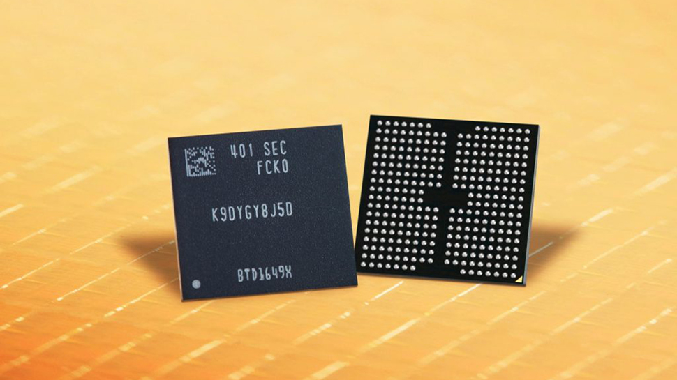
Samsung is working to launch a record-breaking 400-layer vertical NAND flash chip by 2026, reports have claimed.
A report by the Korea Economic Daily says Samsung’s Device Solutions (DS) division aims to advance the NAND flash market with its cutting-edge V10 NAND, designed to meet surging demand in AI data centers.
The company’s memory roadmap, as outlined in the report, shows plans for an advanced 10th-generation NAND that will utilize bonding technology to separately build memory cells and the peripheral circuitry on different wafers, later fusing them into a single chip. Known as bonding vertical NANDFlash (BV NAND), this new approach minimizes heat buildup and maximizes both capacity and performance, creating what Samsung has described as a “dream NAND for AI.”
1,000 layers by 2030
The BV NAND design, boasting a 1.6x increase in bit density per unit area, supports ultra-high-capacity solid-state drives (SSDs) ideal for AI applications.
Samsung’s current 286-layer V9 NAND chips marked a significant milestone, but the 400-layer V10 is expected to redefine capacity limits, potentially breaking the 200TB storage threshold for ultra-large AI hyperscaler SSDs, while improving energy efficiency.
For future releases, world’s largest memory chipmaker plans to introduce 11th-generation V11 NAND in 2027 with a 50% faster data transfer speed, further optimizing performance for high-demand data storage needs.
Samsung’s ambitious NAND roadmap extends even further, with plans for chips exceeding 1,000…
Read full post on Tech Radar
Discover more from Technical Master - Gadgets Reviews, Guides and Gaming News
Subscribe to get the latest posts sent to your email.


