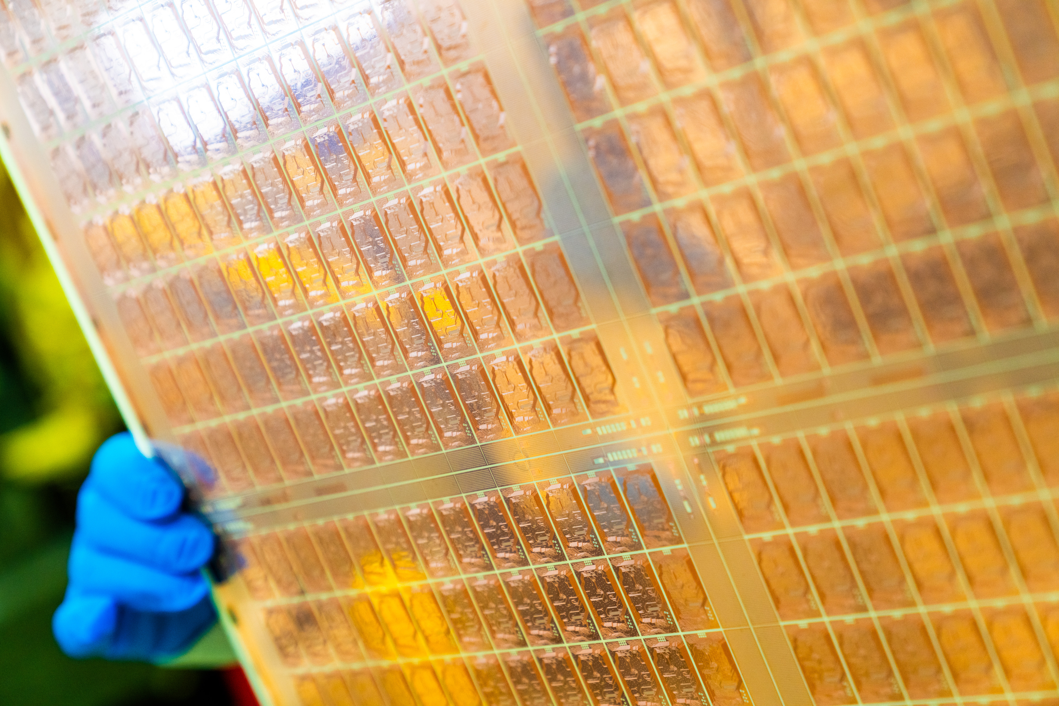
AMD has been granted a patent (12080632) that covers glass core substrate tech. Glass substrates will replace traditional organic substrates for multi-chiplet processors in the coming years. The patent not only means AMD has worked on appropriate technologies extensively but will enable the company to use glass substrates in the future without risks that a patent troll or competitors could sue it.
Most chipmakers, including Intel and Samsung, are exploring glass substrates for future processors. Although AMD no longer produces its own chips, instead subcontracting them out to TSMC, it still has silicon and chip production research and development operations as the company customizes process technologies offered by its partners to build its products.
Glass substrates are made from materials like borosilicate, quartz, and fused silica, which provide notable benefits compared to traditional organic materials as they feature exceptional flatness, dimensional stability, and superior thermal and mechanical stability. Superior flatness and dimensional stability can improve lithography focus for ultra-dense interconnects in advanced system-in-packages, whereas superior thermal and mechanical stability makes them more reliable for high-temperature, heavy-duty applications like data center processors.
One of the challenges when working with glass substrates is the implementation of Through Glass Vias (TGVs), according to the AMD patent. TGVs are vertical pathways created within the glass core to transmit data signals and power. Techniques such as laser drilling, wet etching, and magnetic self-assembly are utilized to produce these vias, but for now, laser drilling and magnetic self-assembly are fairly novel technologies.
Redistribution layers — which route signals and power between the chip and external components using high-density interconnections — are another integral component of advanced chip packages. Unlike main glass core substrates, these will continue to use organic dielectric materials and copper; only this time will they be constructed on one side of the glass wafer, requiring a new production method.
The patent also describes a method for bonding multiple glass substrates using copper-based bonding (instead of traditional solder bumps) to ensure strong, gap-free connections. This approach enhances reliability and eliminates the need for underfill materials, making it suitable for stacking multiple substrates.
While AMD’s patents clearly state that glass substrates offer such benefits as better thermal management, mechanical strength, and improved signal routing capabilities, which are advantages for data center processors, the patent implies that glass substrates could be applied to a variety of applications requiring high-density interconnections, including data center, mobile devices, computing systems, and even advanced sensors, which seems a bit overkill.
Read full post on Tom’s Hardware
Discover more from Technical Master - Gadgets Reviews, Guides and Gaming News
Subscribe to get the latest posts sent to your email.


