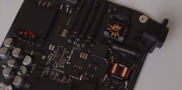
It is astonishing how Apple employed a truckload of techniques to reduce the footprint of its redesigned Mac mini, and the company never bothered to talk in-depth on how it achieved this feat. Then again, the Cupertino giant did not need to, not when curious YouTubers got a hand on these units and performed the disassembly. One of them noticed that the power supply unit’s PCB has separate cutouts so that the components can pass through those openings instead of being soldered on the top, which helps save space, but it is also an expensive process.
The exact figure not mentioned on how much it would cost Apple to make separate cutouts for each Mac mini power supply, but it is the same approach the company took for the more expensive Studio Display
Apart from sporting a design that has no equal, the Mac mini’s power supply unit has components that have been meticulously placed and horizontally aligned to save space. However, YouTuber Quinn Nelson, who runs the channel Snazzy Labs, discovered the cutouts on the PCB and mentioned that it is an incredibly advanced and pricey technique to help reduce the product’s footprint. The same approach was applied to the Studio Display, but the latter is incredibly expensive compared to the $599 starting price of the Mac mini.
There are other ways that helped Apple successfully reduced the Mac mini’s size, such as moving the power button to the bottom of the chassis, which the company’s executives state is not such a big deal because all that is required is tucking the finger to power it on….
Read full on Wccftech
Discover more from Technical Master - Gadgets Reviews, Guides and Gaming News
Subscribe to get the latest posts sent to your email.


